- 您现在的位置:买卖IC网 > Sheet目录336 > IXDI604SI (IXYS Integrated Circuits Division)IC GATE DVR 4A INV 8-SOIC
I NTEGRATED C IRCUITS D IVISION
1 Specifications
IXD_604
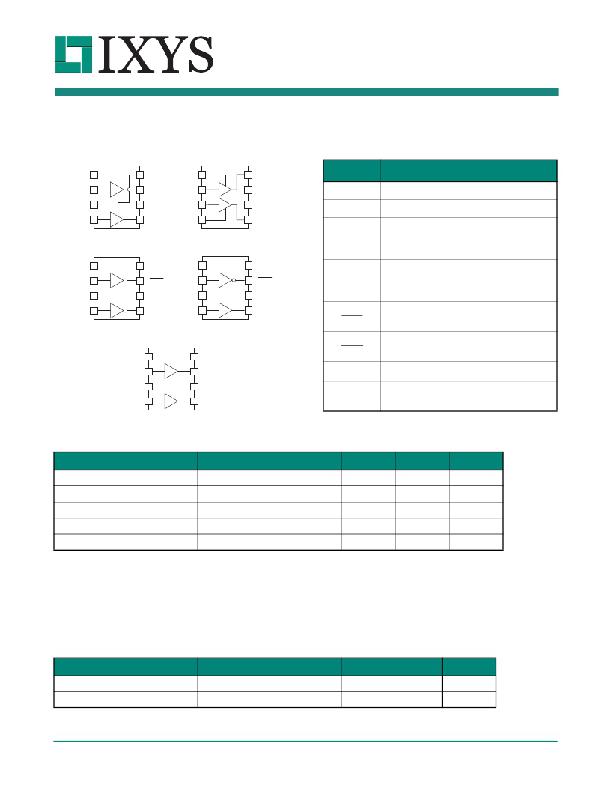
1.1 Pin Configurations
IXDD604PI/SI/SIA
IXDD604D2
1.2 Pin Definitions
E N A
1
8
E N B
E N A
1
8
OUTA
Pin Name
Description
I N A
G N D
I N B
2
3
4
A
B
7
6
5
OUTA
V CC
OUTB
I N A
I N B
E N B
2
3
4
A
B
7
6
5
G N D
V CC
OUTB
INA
INB
Channel A Logic Input
Channel B Logic Input
Channel A Enable Input -
ENA
Drive pin low to disable Channel A and force
IXDI604PI/SI/SIA
IXDF604PI/SI/SIA
Channel A Output to a high impedance state
N C
1
8
N C
N C
1
8
N C
Channel B Enable Input -
I N A
2
A
7
OUTA
I N A
2
A
7
OUTA
ENB
Drive pin low to disable Channel A and force
G N D
3
6
V CC
G N D
3
6
V CC
Channel A Output to a high impedance state
I N B
4
B
5
OUTB
I N B
4
B
5
OUTB
OUTA
Channel A Output - Sources or sinks current to
OUTA
turn-on or turn-off a discrete MOSFET or IGBT
IXDN604PI/SI/SIA
OUTB
Channel B Output - Sources or sinks current to
N C
1
8
N C
OUTB
turn-on or turn-off a discrete MOSFET or IGBT
I N A
G N D
I N B
2
3
4
A
B
7
6
5
OUTA
V CC
OUTB
V CC
GND
Supply Voltage - Provides power to the device
Ground - Common ground reference for the
device
1.3 Absolute Maximum Ratings
Parameter
Supply Voltage
Input Voltage
Output Current
Junction Temperature
Storage Temperature
Symbol
V CC
V INx , V ENx
I OUT
T J
T STG
Minimum
-0.3
-5
-
-55
-65
Maximum
40
V CC +0.3
±4
+150
+150
Units
V
V
A
°C
°C
Absolute maximum electrical ratings are at 25°C
Absolute maximum ratings are stress ratings. Stresses in excess of these ratings can cause permanent damage to the device.
Functional operation of the device at conditions beyond those indicated in the operational sections of this data sheet is not
implied.
1.4 Recommended Operating Conditions
Parameter
Supply Voltage
Operating Temperature Range
R05
Symbol
V CC
T A
www.ixysic.com
Range
4.5 to 35
-40 to +125
Units
V
°C
3
发布紧急采购,3分钟左右您将得到回复。
相关PDF资料
IXDI609YI
IC GATE DVR 9A DUAL HS TO263-5
IXDN402SIA
IC MOSFET DRVR DUAL 2A 8-SOIC
IXDN414YI
IC DRIVER MOSF/IGBT 14A 5-TO-263
IXDN509D1T/R
IC GATE DRIVER SGL 9A 6-DFN
IXDN514SIAT/R
IC GATE DRIVER SGL 14A 8-SOIC
IXDN602PI
MOSFET N-CH 2A DUAL LO SIDE 8-DI
IXDN630CI
IC GATE DRIVER LOW SIDE 5TO220
IXDS430SI
IC DRVR MOSF/IGBT 30A 28-SOIC
相关代理商/技术参数
IXDI604SIA
功能描述:功率驱动器IC 4A Dual Low-Side Ultrafast Mosfet DRV RoHS:否 制造商:Micrel 产品:MOSFET Gate Drivers 类型:Low Cost High or Low Side MOSFET Driver 上升时间: 下降时间: 电源电压-最大:30 V 电源电压-最小:2.75 V 电源电流: 最大功率耗散: 最大工作温度:+ 85 C 安装风格:SMD/SMT 封装 / 箱体:SOIC-8 封装:Tube
IXDI604SIATR
功能描述:功率驱动器IC 4A Dual Low-Side Ultrafast Mosfet DRV
RoHS:否 制造商:Micrel 产品:MOSFET Gate Drivers 类型:Low Cost High or Low Side MOSFET Driver 上升时间: 下降时间: 电源电压-最大:30 V 电源电压-最小:2.75 V 电源电流: 最大功率耗散: 最大工作温度:+ 85 C 安装风格:SMD/SMT 封装 / 箱体:SOIC-8 封装:Tube
IXDI604SITR
功能描述:功率驱动器IC 4A Dual Low-Side Ultrafast Mosfet DRV
RoHS:否 制造商:Micrel 产品:MOSFET Gate Drivers 类型:Low Cost High or Low Side MOSFET Driver 上升时间: 下降时间: 电源电压-最大:30 V 电源电压-最小:2.75 V 电源电流: 最大功率耗散: 最大工作温度:+ 85 C 安装风格:SMD/SMT 封装 / 箱体:SOIC-8 封装:Tube
IXDI609CI
功能描述:IC GATE DVR 9A NON-INV TO220-5 RoHS:是 类别:集成电路 (IC) >> PMIC - MOSFET,电桥驱动器 - 外部开关 系列:- 标准包装:5 系列:- 配置:低端 输入类型:非反相 延迟时间:600ns 电流 - 峰:12A 配置数:1 输出数:1 高端电压 - 最大(自引导启动):- 电源电压:14.2 V ~ 15.8 V 工作温度:-20°C ~ 60°C 安装类型:通孔 封装/外壳:21-SIP 模块 供应商设备封装:模块 包装:散装 配用:BG2A-NF-ND - KIT DEV BOARD FOR IGBT 其它名称:835-1063
IXDI609PI
功能描述:IC GATE DVR 9A NON-INV 8DIP RoHS:是 类别:集成电路 (IC) >> PMIC - MOSFET,电桥驱动器 - 外部开关 系列:- 标准包装:50 系列:- 配置:低端 输入类型:非反相 延迟时间:40ns 电流 - 峰:9A 配置数:1 输出数:1 高端电压 - 最大(自引导启动):- 电源电压:4.5 V ~ 35 V 工作温度:-40°C ~ 125°C 安装类型:表面贴装 封装/外壳:TO-263-6,D²Pak(5 引线+接片),TO-263BA 供应商设备封装:TO-263 包装:管件
IXDI609SI
功能描述:IC GATE DVR 9A NON-INV 8SOIC RoHS:是 类别:集成电路 (IC) >> PMIC - MOSFET,电桥驱动器 - 外部开关 系列:- 标准包装:50 系列:- 配置:低端 输入类型:非反相 延迟时间:40ns 电流 - 峰:9A 配置数:1 输出数:1 高端电压 - 最大(自引导启动):- 电源电压:4.5 V ~ 35 V 工作温度:-40°C ~ 125°C 安装类型:表面贴装 封装/外壳:TO-263-6,D²Pak(5 引线+接片),TO-263BA 供应商设备封装:TO-263 包装:管件
IXDI609SIA
功能描述:IC GATE DVR 9A NON-INV 8SOIC RoHS:是 类别:集成电路 (IC) >> PMIC - MOSFET,电桥驱动器 - 外部开关 系列:- 标准包装:50 系列:- 配置:低端 输入类型:非反相 延迟时间:40ns 电流 - 峰:9A 配置数:1 输出数:1 高端电压 - 最大(自引导启动):- 电源电压:4.5 V ~ 35 V 工作温度:-40°C ~ 125°C 安装类型:表面贴装 封装/外壳:TO-263-6,D²Pak(5 引线+接片),TO-263BA 供应商设备封装:TO-263 包装:管件
IXDI609SIATR
功能描述:IC GATE DVR 9A NON-INV 8SOIC RoHS:是 类别:集成电路 (IC) >> PMIC - MOSFET,电桥驱动器 - 外部开关 系列:- 标准包装:50 系列:- 配置:低端 输入类型:非反相 延迟时间:40ns 电流 - 峰:9A 配置数:1 输出数:1 高端电压 - 最大(自引导启动):- 电源电压:4.5 V ~ 35 V 工作温度:-40°C ~ 125°C 安装类型:表面贴装 封装/外壳:TO-263-6,D²Pak(5 引线+接片),TO-263BA 供应商设备封装:TO-263 包装:管件
